
In the picture above, the “Ugly” style of construction can plainly be seen. The benefits are the rapidity of construction and the advantage of the continuous RF ground plane provided by the PC board surface the components are added to.
Since this picture was taken, RIT has been added to the VXO, taking the place of a simple switched capacitance Tx frequency offset scheme. The RIT pot is now in the location of the push-button switch shown here. The push-button switch, used to program the Tick keyer, and a “spot” switch are now mounted below the RIT pot in the front panel.
What started out as a simple VXO experiment has snowballed into the building of a complete 10 Meter QRP CW Transceiver. The rig tunes from 28.001 through 28.088 MHz, covering a good portion of the lower end of the band and including both the common DX frequencies and the 10 Meter QRP calling frequency.
A 14 MHz VXO, followed by a frequency doubler and a double-tuned bandpass filter, provides a stable 28 MHz signal source for the transmitter, and, with a frequency offset scheme utilizing RIT, acts as the direct conversion receiver’s local oscillator as well.
Because of the inherent non-linearity of a wide-band VXOs tuning, the RIT is not linear across the tuning range. However, the RIT circuit shifts the 28 MHz signal 1 KHz at the upper end of the VXOs’tuning range and about 2.7 KHz at the low end. In practice, this has proven to be sufficient, as it is easy to adjust the RIT knob for whichever received tone is preferred by first zero beating the received signal through the use of the “spot” switch and then adjusting the RIT as desired.
The transmitter puts out about 1.5 Watts, and the receiver, a simple direct conversion design lifted from Wes Hayward, W7ZOI’s, updated Micro Mountaineer, is sensitive enough to hear all but the weakest of signals.
A Tick keyer was included, both to provide the keying function and to provide sidetone, which is introduced into the receiver’s audio output.
I started out working with a simple crystal oscillator, using a common 2N2222 and a pair of 14.060 MHz crystals. After a bit of experimentation, and switching from a pair of cheap silicon diodes to a 1SV149 tuning diode, the VXO tuned from 13.990 through 14.044 MHz. The addition of a resistor in the ground lead of the tuning pot, selected in value to set the lower end of the tuning range just above 14000.5 KHz, prevents out-of-band operation.
Obviously, the fundamental tuning range of this VXO would be quite useful on 20 Meters, as well, but since I had already built a push-push frequency doubler for another project, and had wanted to try QRP on the 10 Meter band, I chose to use the VXO as part of an all homebrew Ten Meter CW rig.
Although the peak of the sunspot cycle has passed, there are still sufficient band openings and enough activity to warrant putting the rig on 10 Meters, and on-the-air results have more than justified the small amount of work and low cost of building the rig. Since I keep a fairly extensively stocked “junk box” of parts, I had all the parts needed for the rig already on hand.
Once the RIT circuit was added to the VXO, the signal was routed to a JFET buffer amp and push-push frequency doubler, on to a driver stage utilizing the metal case 2N2222A, and then to a single-ended power amplifier using a cheap and readily available 2N3053.
However, there were a couple of drawbacks to overcome. First and foremost, the signal purity was not good. Too much of the fundamental was getting through the transmitter, no matter how carefully the push-push frequency doubler was balanced. And, although the three quarters of a watt a single 2N3053 produced is sufficient power output for many contacts on 10 Meters, the PA transistor was running too hot.
Adding a double-tuned bandpass filter between the frequency doubler and the driver stage cleaned up the signal nicely. Adding a second 2N3053 in parallel with the existing PA gave about a Watt and a half of power output and cool running of the transistors.
With the transmitter basically finished, and having a 28 MHz local oscillator signal readily available, the addition of a Direct Conversion receiver to turn the rig into a complete transceiver was a natural. Having wanted to try out the simple receiver design by Wes Hayward, W7ZOI, published in his July 2000 QST article on an updated Micro Mountaineer, I welcomed the opportunity to couple that receiver with the finished transmitter.
In my conversion of an SMK-1 to 20 Meters, I had found that an RF preamp was a necessary addition if one were to reliably hear weak signals on that band, with the NE602 and LM386 in a configuration similar to the MRX40 receiver. Wes, W7ZOI, had reported in his article on the updated Micro Mountaineer that the simple NE602/LM386 receiver in his rig copied a .1 uV signal. This was the primary factor resulting in the choice of using his design in this rig for 10 Meters. If the addition of an RF Preamp for the receiver was unnecessary, the rig could be kept simpler.
The SA612 Mixer is still manufactured by Phillips, and the other parts and transistors used to build the rig are commonly and cheaply available. Many of the parts are available from your local Radio Shack store.
All resistors used are ¼ Watt. All the .1 bypass caps in the rig are monolithic. The .01s and .001s used were disk ceramic. NP0 caps were used in all the frequency determining parts of the rig, and Silver Micas were used in the transmitter’s output filter. I have not included a parts list, but with each stage individually detailed, a parts list is easily made up as construction progresses, stage by stage.
The Circuits
The complete transceiver’s circuit is divided into three parts, here, for easier viewing. The three sections are designated VXO and Doubler, Filter and Transmitter, Receiver and Keying.
- Here is the schematic of the VXO, Buffer and Frequency Doubler
- Here is the schematic of the Double-Tuned Bandpass Filter and Transmitter
- And finally the schematic of the Receiver and Keying circuitry
Building The Rig
Except for the few Manhattan style pads glued down in order to mount a socket for the SA612 mixer IC, those few that are used to insulate contacts of the various trimmer capacitors, and a few in the Tick Keyer circuit, the entire remainder of the rig was easily and quickly built “Ugly” style, over the continuous copper ground plane of single sided PC board. If you have not yet tried this method of building, let me just say that this is the easiest and fastest building method I have used. That, coupled with the fact that RF circuits built this way operate better and cleaner over that continuous copper ground plane than they do in a PC board, makes “Ugly” even better.
Sure, I know there is no PC board and photo layout to follow. You just start at the natural beginning of a circuit, in this case the VXO, start with a part that solders directly to ground, such as the 1 K resistor in the emitter lead of the VXO transistor, cut one lead, bend it at 90 degrees, solder it to the ground plane with the body of the resistor standing straight up, and continue installing parts, alternating between the legs of parts that go to ground and legs of parts that attach to the upper legs of parts that are grounded. You will be amazed at how fast and easy this is, and who cares if it isn’t perfectly symmetrical or if there is no part label on the “PC” board.
If you run out of room in one direction on your PC board base, turn the corner and keep going. Or build part of the circuit on another board and tack solder them together. Think of how small a rig you can build if you put part of the circuit on the bottom, part on the sides, and part on the top of an all PC board equipment case.
Because you have the choice of either building the complete circuit on one continuous sheet of PC board material that will end up being the bottom of your PC board material case, or building the circuit in sections, on small pieces of PC board material that can be tack soldered wherever your layout requires, this method is very flexible and lends itself quite readily to circuit changes, especially at the stage and module level.
Short pieces of hookup wire form the 12 Volt supply lines, and either short pieces of shielded wire or hookup wire connect the controls, switches, and the RF, power and earphone connectors to the circuit.
No high value resistors were used as standoff insulators, and no insulated soldering pads cut from PC board were needed other than those few previously mentioned. There are enough parts soldered directly to ground, and there is enough rigidity in part leads, to ensure that the components are mechanically stable without their use.
The main tuning pot, the RIT and RF Gain controls, and the two push-button switches for programming the Tick Keyer and Spotting the transmitter frequency are mounted on the front panel. The rear panel has the power connector, BNC RF output jack, and the paddle and headphone jacks.
The drawing below shows the general layout of the circuit as built on the PC board bottom of the case. Only the Tick keyer is on a small, separate board, which is tack soldered vertically to the rear panel of the PC board case.

Here is a photo of the rig, showing the same layout:

In this layout, the finished size of each section is entirely up to the builder, as is the finished size of the whole. With this layout, the signal starts in the VXO, goes to the Buffer and Frequency Doubler, through the Double Tuned bandpass filter, and from there to both the transmitter driver and the receiver mixer. The input side of the transmitter driver faces the DT filter, as does the mixer side of the receiver, facilitating easy connections.
Use silver content solder, both for the stronger and cleaner solder joints it makes and for the reduction in lead exposure. I use two soldering irons of differing wattages, a low wattage iron for attaching parts to each other, and a medium wattage iron for soldering either parts or PC board sections to the PC board base. There is no need to bend part leads around each other. They should be touching, and the nice clean flow of a small amount of solder should cover their junction. If the first two parts are joined in this manner, it is easy to re-heat the joint and add each next part lead. You will quickly learn that having the far end of previously installed parts already soldered to their adjoining parts will prevent the junction you want to add to from falling all apart when you re-flow the solder.
Here is a general layout of the VXO section of the “board”.

Build the VXO first, starting with the oscillator itself, from the emitter up. Leave about ¾” of free space on the board to the left of the VXO, which will be the front of the rig, so that the parts will clear the tuning pot and other controls.
Here is the circuit of the VXO:

Here is a picture of the VXO:

Once the oscillator is built, including its voltage regulator, the “ground” leg of the tune pot, or a substitute, can be soldered directly to the edge of the board, the wiper is connected to the 10 K resistor leading to the tuning diodes, the top leg of the pot is connected to the top of the 9.1 volt Zener, and the oscillator can be tested. Either listen for its output in a receiver, or check its output with an RF voltmeter and frequency counter, at the emitter of the transistor.
The signal should be quite strong in a nearby receiver, and with the components listed, you should get 40 KHz or more of tuning range.
In my rig, the initial tuning range was 13.990 to 14.044 MHz. I put a 12 K resistor between the ground leg of the Tune pot and ground in order to fix the lower end of the tuning range just above the bottom of the band.
However, wait until the RIT circuit is installed before installing R-Adj, as it is labeled in the RIT Circuit, as that will slightly change the tuning range of the VXO.
Once you are satisfied the VXO is working properly, disconnect the power source and install the entire RIT circuit, beginning with the 15 pf cap that attaches at the junction of the oscillator transistor’s emitter and the tops of the 1 K resistor, and the 33 and 10 pf caps. For the time being, the cathode of the 1N914 that will attach to the “key” line is left floating, unconnected.
Here is the RIT circuit:

Solder a cutoff part lead to one end leg of the RIT pot, and solder a couple of three inch long pieces of hookup wire to the other two legs. This way, the RIT pot can be connected to the circuit in order to test the RIT and TX frequency offset functions.
The wiper of the pot connects to the cathode end of the 15 Volt Zener used in the RIT circuit. The leg of the pot opposite the ground leg is connected to 9.1 volts regulated at any convenient spot in the oscillator circuit.
Once the RIT pot is connected, apply 12 volts to the VXO circuit again, either hook a frequency counter up to the emitter of the oscillator transistor or listen to the second harmonic of the VXO in a nearby receiver, and check the function of the RIT. At the low end of the VXO tuning range, the RIT should change the 28 Mhz harmonic a total of about 2.7 KHz. At the upper end, it should provide about 1 KHz of total frequency change.
Then, with the RIT pot centered in its travel and the VXO at the low end of its tuning range, use a test lead with alligator clips on each end to ground the cathode of the 1N914 that will eventually connect to the “Key” line. With it grounded, the VXO frequency should shift, and in this case about 1 KHz or so.
The exact amount of frequency shift depends on the position of the RIT control. At one end of the RIT knob’s travel, there will be no frequency shift when the key line is grounded. At the other end of the RIT pot’s travel, with the VXO at the low end of its tuning range, the frequency will shift about 2.7 KHz.
In my rig, the Tune pot is connected so that the VXO’s frequency goes up as the pot is rotated clockwise, and the RIT pot is connected so that no shift occurs when the pot is turned all the way clockwise.
In practice, if one desires to listen to the same received tone throughout the entire tuning range of the rig, the received signal is zero beat while holding the “spot” push-button switch in, and then the “spot” switch is released and the RIT knob adjusted for the desired reception tone.
With this arrangement, popularized by Roy Lewallen, W7EL, in his “Optimized QRP Rig”, one listens to the upper sideband of any received signal, in order to place the offset transmitter signal on frequency in the other person’s receiver. Holding the “Spot” switch in while tuning the received signal to zero beat will ensure that the transmitted signal is exactly on the received frequency. Substituting a SPST toggle switch may make tuning easier, as the RIT can be switched off while tuning, then switched back on, without having to hold a push-button style switch in while doing so.
Now that the RIT Circuit is installed and working, it is time to install the resistor, Radj, that determines the lower end of the tuning range. Assuming your VXO tunes below the bottom of the band, R-Adj will be needed so as to prevent out-of-band transmissions.
While either monitoring with another receiver or with a Frequency Counter, tune the VXO just above the bottom of the 20 Meter band, say around 14000.5 KHz. Disconnect the power from the VXO, unsolder the wire connected to the wiper of the Tune pot, and, being sure not to turn its knob, measure the resistance from the wiper leg of the pot to ground. The resistance measured will be very close to that amount needed to keep the VXO from tuning below the bottom of the band. Install the next larger common value of ¼ Watt resistor between the ground leg of the pot and ground, and re-connect the wire to the wiper.
Test the tuning range of the VXO to be sure it doesn’t tune below 14000.0 Khz. As we will be transmitting the upper sideband of the VXO frequency, doubled to 28 MHz, this will ensure that we stay within the band with our transmitted signal. Just to be sure, re-check the low end of the tuning range while listening to the 28 MHz harmonic of the VXO.
Add the keying circuitry next, in its designated general area in the VXO section of the “board”.
Here is the keying circuit:

In actuality, the 12 Volt “Bus” wiring will eventually run directly from the 12 Volt power jack to the PA stage and then on to the other various stages that require it, so, at present, the 12 Volt connection shown here is the same point as the 12 Volt connection for the VXO. The 12 Volts Keyed line to the driver will be added after that stage is built.
Once the keying circuitry is built, and 12 Volts applied, it can be tested by measuring the voltages on the Collectors of both keying transistors, as it will be 0 Volts when the rig is in “Receive” mode, and 12 volts when the Key line is grounded in “Transmit” mode.
The Key line connection shown here is connected to the Key line contact in the RIT circuit, and will be connected to the Key line contact in the Tick Keyer circuit, once that is built and added to the rig.
Next, build the JFET buffer amp and the Frequency Doubler. Here is the circuit:
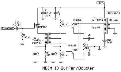
The general layout for the JFET buffer amp, Push-Push pull frequency doubler and double-tuned bandpass filter is as follows:

Here is a picture of the buffer and frequency doubler:

Once the buffer and frequency doubler are built, test this stage. Bare necessity test equipment for use in this project should include an oscilloscope, a high impedance voltmeter with RF probe, a receiver capable of receiving both the 20 Meter and 10 Meter ham bands, and a 50 Ohm resistive dummy load. A wattmeter helps, but the voltmeter and RF probe will suffice if one is unavailable.
If you don’t own an oscilloscope or other pieces of necessary test gear, a nearby ham should be more than glad to help you test and align stages as they are added to the circuit. I certainly extend that invitation to anyone in my area who wishes to build any gear that I can help with.
An oscilloscope is definitely a plus when alignment and adjustment of the push-push frequency doubler is performed, as one first adjusts the trimmer in the doubler output for maximum 28 MHz signal, and then adjusts the balance pot between the emitters of the push-push transistors for a minimum or null of the 14 MHz fundamental.
Either a 51 or 47 Ohm resistor is connected temporarily from the top of the 3 turn link to ground, and the signal monitored there. Once this section is aligned, DC power is disconnected and the resistor is removed.
The double tuned bandpass filter is built next, up to and including the 51 Ohm resistor which serves as its load. Here is its circuit:

The double-tuned bandpass filter can be seen in the upper center of this photo:

After re-connecting DC power, the filter is aligned by adjusting the two trimmers for maximum 28 MHz signal, and minimum 14 MHz fundamental, while observing the signal at the top of the 51 Ohm resistor at the output, on an oscilloscope. This adjustment should be performed with the VXO tuned to the center of its tuning range, so as to provide a more uniform signal level throughout the entire tuning range.
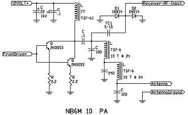
Build the driver stage next, including the 22 Ohm resistor that goes from the top of the 3 Turn link on its output transformer to ground. Here is its circuit:

The Driver, PA, Output Filter, Receiver Tuned input Circuit general layout is pictured below:

A picture of the driver and part of the PA circuit is here:

The trimmer shown at center left is not needed in the driver, and is not included in the circuit diagram, as it was removed after this photo was taken.
Connect the 12 Volts Keyed line to the collector of Q6 in the keying circuit. Connect the 12 Volt DC supply line, and test the driver by either listening for an increase in 28 MHz signal in a receiver, by observing the output with a voltmeter and RF probe, or with an oscilloscope while grounding the Key line.
The PA stage and its output filter is built next, and connected to the BNC antenna jack. Include the trimmer TC1 and the two QSK diodes, D1 and D2 in the area of the output filter. Use heat sinks on the 2N3053 transistors.
The PA and output filter circuit is here:
At this point, the transmitter is complete, and can be tested, by grounding the Key line while the transmitter is connected to a Wattmeter and Dummy Load, or while the output is monitored with Voltmeter and RF probe or Oscilloscope while connected to a Dummy Load. The prototype rig’s transmitter produces about 1.5 Watts of output.
Next is the receiver. Here is the general layout for the receiver and its muting circuitry:

The circuit of the receiver’s Mixer and muting transistors is pictured below:

When it is finished, be sure to connect the mute line to the top of the 1 K resistor in the Keying Circuit, at the point labeled “Mute”, and connect the 10 pf cap from pin 6 of the IC to the top of the 51 Ohm resistor in the output of the DT filter.
The Receiver Audio amp circuit follows:

A picture of the Receiver section of the rig is here:

The IC and circuitry on the small vertical piece of PC board is the Tick Keyer.
The RF Gain pot will be mounted on the front panel. Use shielded wires to connect it to both the RF input and the Receiver Mixer.
When the receiver section is complete, with the 12 Volt supply line connected and with an earphone jack connected between the AF output and ground, the receiver can be aligned and tested.
The earphone jack should be wired so that the AF output goes to the “tip” connection of the stereo earphone jack, and the ground connection goes to the “ring” connection. When the jack is installed in the rear panel of the case, enough of the copper surface is scraped off both the inside and outside surfaces of the panel so that the “ground” connection of the jack is NOT grounded. Wiring the earphone jack this way provides higher audio output from the stereo earphones, as they are connected in series.
With a 10 Meter antenna attached, and while listening to a weak signal, or background noise in the absence of a signal, adjust TC1 and TC2 for maximum signal or noise level.
This receiver is prone to hum when it is out of a case, especially at the highest RF Gain settings. The hum should disappear or be greatly reduced when the rig is enclosed in a shielded case, and the hum can be carefully tuned out or much reduced, if still there, by careful adjustment of TC1 and TC2 in order to achieve best signal level with the least amount of hum. The last section to be built is the Tick keyer.
Here is the Tick keyer circuit:

I built the keyer circuit on a small piece of double sided PC board that I tack soldered vertically to the inside surface of the rear of the case, near the top, between the Paddle jack and DC Power jack. This facilitated making its connections to the Paddle jack, receiver audio stage, and to the 5 Volt regulator. A piece of hookup wire connects the collector of the keying transistor to the Key line in the keying circuit.
Now it is time to build the front and rear panels of the case, and ensure that all the connections between stages are properly made.
Use the three general circuit diagrams as a guide to make sure all interconnecting lines are properly installed.
Here is a drawing of the NB6M 10’s front panel arrangement:

The rear panel layout is as shown here:

The actual size of these panels is determined by the finished size of your layout, and can be cut accordingly. Use double sided PC board for the front and rear panels, and install them about an eighth of an inch inside the edge of the PC board base, so that they can be tack soldered on both the inner and outer bottom edges.
Before installing the side panels, make all connections to the various jacks, switches and potentiometers.
Then, cut and install the side panels, tack soldering them to the front and rear panels. Once the side panels are installed, and all final connections made, Readjust TC1 and TC2 in the receiver circuit for maximum signal gain and minimum or no hum.
Cut and install the top of the case, tack soldering it to the front and rear panels, and the rig is ready to use.
Final Thoughts
Although it is nearly impossible to exactly duplicate the layout of a circuit that is built “Ugly” style, it should be noted that exact duplication is not necessary. Stages can be built on individual pieces of PC Board, or not, as the builder desires. The size of the project is also up to the builder. If one is used to building only on PC boards, with exact parts placement, this may seem daunting. However, ease and rapidity of construction coupled with clean RF operation of the circuitry and flexibility of layout and final project size and shape more than make up for the lack of a PC board and exact parts layout.
As always, building any project stage by stage, and testing each stage as you go, helps a lot.
This rig could certainly benefit from a more refined receiver. However, adding a simple DC receiver made this transceiver come together quickly and easily, and this receiver is adequate for many contacts. A DC receiver capable of single signal reception, such as the Mini-R2 would be a great alternate choice.
None of the parts used are unique or exotic. While the SA612 mixer ICs are getting scarce, with only Phillips manufacturing them, they are still available.
It is interesting how one simple ham radio experiment leads to so much more, in this case resulting in a fun little rig for a band that is not receiving as much attention, operation wise, as it should. In the short time since building the rig, contacts have been made across the United States and Canada, and several exciting DX contacts, including several in Europe, have been made as well.
It is my hope that some of the ideas presented here in this rig will provide the impetus for building projects of your own. The rewards, both in terms of learning and in the simple joy of operating a rig that you have built from scratch yourself, are well worth the effort.